355nm UV 레이저 마킹 휴대폰 칩, 휴대폰 케이스
Aug 14 , 2022355nm UV laser marking mobile phone chip, mobile phone case
Thanks to the continuous exploration and application of new materials and new processes, the speed of upgrading of smartphones is overwhelming. Among them, the laser marking process is of great significance, clean and pollution-free, with high marking clarity, never falling off, and empowering smartphones. Manufacturing quality and efficiency.
The principle of laser marking is that the high-energy density laser beam acts on the designated area of the material to rapidly melt and vaporize the surface material, and the beam movement path can be set according to the computer, and finally the required graphic mark is formed. Laser marking is not limited to material planes, but can also be marked on special-shaped surfaces, and is suitable for marking on metals, plastics, glass, ceramics, polymers, wood, paper and other materials.
So, where does the smartphone use laser marking? Bearing the brunt of the marking of mobile phone casings, the use of laser marking on mobile phone casings is now a routine operation. As the most intuitive part of consumers, the mobile phone case/shape has too many expectations. For this reason, mobile phone manufacturers will mark their own brand logo and other text, numbers and other information on the back cover of the mobile phone to make it look fashionable and technological. It can also show its own brand characteristics.
There are also many places where laser marking is used inside the mobile phone. Chips and memories are scattered on the motherboard of the mobile phone. In addition to the components such as vibration motors and camera components, these components are characterized by small size and high integration. , The surface area that can be marked is small, and the ink printing method is not environmentally friendly, unrealistic, and not clear and durable enough. The spot after the laser beam is focused is very small, only a few tens of microns, which can realize high-precision, high-resolution, high-density marking in a small range, thus bringing sustainable anti-counterfeiting and traceability functions of chips, memories and other components, Technology is displayed in every square inch.
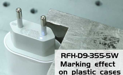
휴대폰 주변 제품에서도 레이저 마킹의 흔적을 흔히 볼 수 있으며 전원 어댑터, 휴대폰 보호 케이스, 데이터 케이블, 블루투스 헤드셋, 헤드폰 케이블 등의 액세서리에 레이저 마킹을 할 수 있습니다. 따라서 휴대폰 제조의 전체 산업 체인에서 레이저 마킹 프로세스는 어디에나 있으며 그 중요성은 자명합니다.
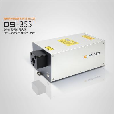
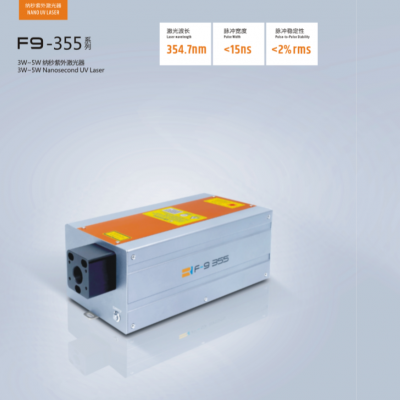
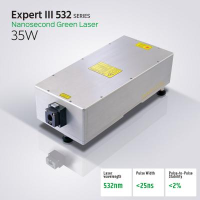
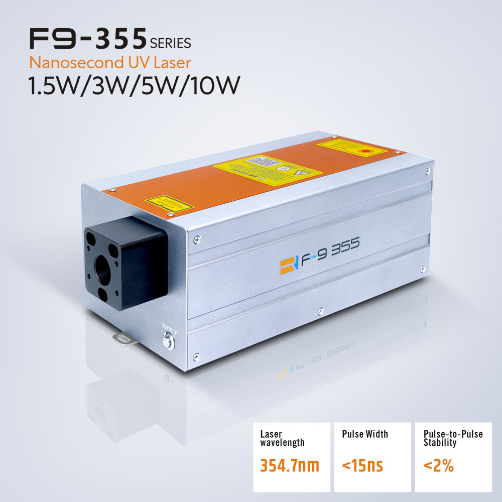
NanoFilm의 355nm UV 나노초 레이저는 작지만 성능이 뛰어납니다. 높은 단일 광자 에너지, 쉬운 포커싱 및 355nm 자외선의 높은 재료 흡수율의 특성은 "냉간" 가공을 위한 레이저 마킹 분야에서 높이 평가되며 마킹 중에 열 영향 영역이 매우 작습니다. 우수한 빔 품질(M2 < 1.2) 포커싱 후면 광점은 작고 작으며 마킹 시 선폭이 좁고 필라멘트와 같은 "나이프"는 독이나 오염 없이 작은 영역을 쉽게 마킹할 수 있습니다.
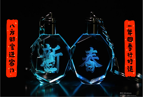
또한 355nm 자외선 나노초 레이저는 필름, 플라스틱, 유리, 실리콘 웨이퍼, 종이 및 기타 재료의 마킹에도 사용할 수 있습니다.