10와트 UV(355nm) 레이저 모듈 마킹 절연 게이트 바이폴라 트랜지스터
Dec 19 , 202210와트 UV(355nm) 레이저 모듈 마킹 절연 게이트 바이폴라 트랜지스터
Insulated Gate Bipolar Transistor의 전체 이름인 IGBT는 말 그대로 Insulated Gate Bipolar Transistor로 번역됩니다. 데이터에 따르면 IGBT의 내전압은 6500V 이상에 달할 수 있고 통과 전류는 수천 암페어에 달할 수 있으며 IGBT는 주파수 변환 모듈로 사용되며 주파수 변환은 초당 수만 번에 달할 수 있습니다.
Thanks to this, IGBT is commonly known as the "CPU" of power electronic devices. It is widely used in rail transit, smart grid, aerospace, electric vehicles, and new energy equipment. It is the core device for energy conversion and transmission, such as used on high-speed rail. The inverter circuit of the new energy electric vehicle Tesla is composed of IGBTs. The battery output of the new energy electric vehicle Tesla is DC, but the motor is AC. At this time, there are IGBT devices at the hub of converting from DC to AC.
Today, IGBT has become an indispensable and important component of photovoltaic and automotive electronics circuits. In order to clarify product-related parameters, manufacturers generally mark product numbers, circuit diagrams, etc. on certain areas of the IGBT. Conventionally, they are marked by labeling or spraying codes. With the expansion of laser marking applications, marking on the surface of the IGBT has also gained Wide application, which is mainly due to the following aspects:
The first is that the marking obtained by laser marking is permanent, does not fall off, does not blur, is resistant to wear and scratches, and can maintain the shape of the mark for a long time, which is of great significance for anti-counterfeiting and traceability; secondly, the marking line of laser marking The width can be on the order of microns, and the markers can be marked with high quality in the tiny area of the IGBT, even barcodes and two-dimensional codes are not a problem; moreover, laser marking makes full use of the flexibility of the computer for graphics and paths Automatic control, high marking efficiency, high consistency of markers, editable, no other consumables, no molds, good subjective initiative; finally, laser marking is non-contact processing, no external force is applied to IGBT, and it is not easy to damage the device, ensuring performance Reliable and stable.
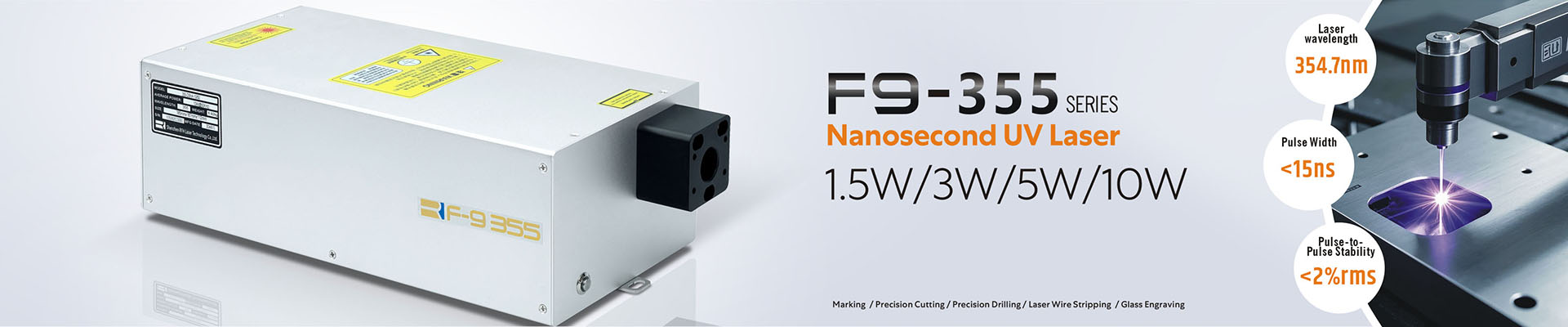
The 355nm UV nanosecond laser has excellent performance in plastic materials, and more and more customers choose it. It has the characteristics of narrow pulse width (about 25ns), fast speed, high precision, high peak value, and easy absorption of materials. It is also called "cold" processing method and can perform marking, cutting, drilling, etching and other processes. Moreover, its beam quality is high (M2<1.2), easy to focus, and the output spot diameter is small, which is one of the key parameters to achieve micron-level line width marking, which is as thin as a hair.
더 중요한 것은 355nm 자외선 레이저의 단일 광자 에너지가 높아 일부 재료의 분자 결합을 파괴할 수 있으므로 재료가 표면층에서 빠르게 기화되고 증발될 수 있습니다. 이것은 광화학 반응입니다. 민감한 플라스틱 소재는 친근하며 마크의 선명도와 외관에 영향을 미치는 타는 것, 탄화, 용융 등을 유발하기 쉽지 않습니다.
오늘날 많은 생산 회사는 레이저 마킹을 위해 조립 라인에 355nm 자외선 레이저를 통합했습니다. 레이저 마킹 기계를 사용하면 코딩이나 라벨링의 한계와 단일성을 해결할 뿐만 아니라 미세 마킹으로 제품의 품질도 향상됩니다. 높은 안정성은 의심할 여지 없이 다운스트림 고객 사이에서 브랜드 품질을 향상시키고 측면에서 치열한 시장에서 제품 경쟁력을 향상시킵니다.