첨단 기술을 보여주는 355 UV 레이저 소스 마킹 PCB 회로 기판
Sep 01 , 2022UV laser marking PCB circuit board, showing high technology
Since the reform and opening up, China has attracted a large-scale transfer of manufacturing in Europe and the United States due to its preferential policies in labor resources, markets, and investment. development of related industries.
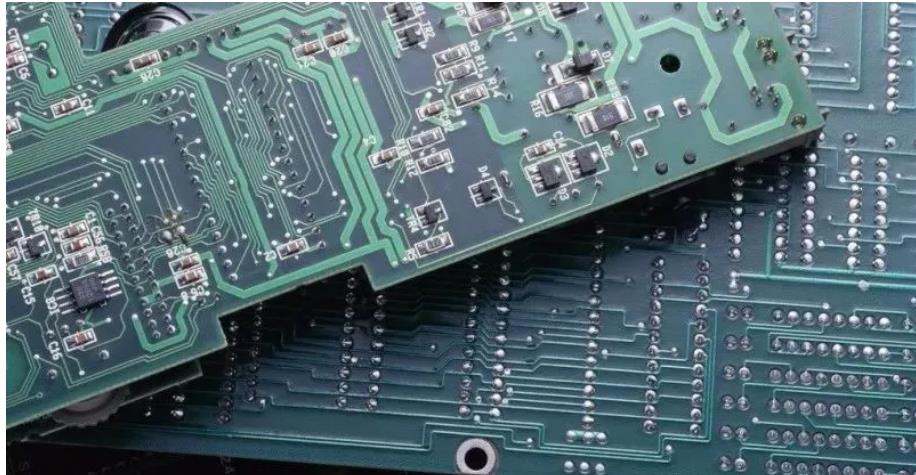
As the "mother of electronic products", PCB circuit board is an important electronic component, the support of electronic components, the carrier of electrical connection of electronic components, and the upstream of almost all electronic consumer goods, whether it is mobile phones, computers, tablets, etc. Display screens, etc., will use circuit boards and have a wide range of applications.
There are two main types of PCB marking processing: silk screen printing and laser marking.
The traditional silk screen printing process is rough, and the logo is easy to fall off, causing inconvenience to the user. In addition, the silk screen processing procedure is cumbersome, and the operator needs to be replaced in time to ensure the production efficiency, which increases the labor cost.
With its accuracy and flexibility, laser marking can make up for the lack of silk screen processing, and gradually become the best processing tool for PCB marking, and will play a pivotal role in the circuit board industry!
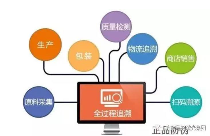
Laser marking technology can skip number marks, realize one code for one item, and mark two-dimensional code on the PCB, which can achieve quality traceability and let users know product information with one click.
▲ Quality traceability
Han's Yueming Laser Group
Marking
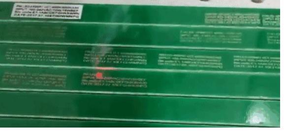
Laser marking is a marking method that uses a high-energy-density laser to locally irradiate the PCB board to vaporize or change the color of the surface material, thereby leaving a permanent mark.
Laser marking can print various characters, symbols and patterns, etc., and the character size can range from millimeters to micrometers, which is of special significance to the anti-counterfeiting of products.
What is the special laser marking machine for PCB?
What about "sparkle"?
High precision: Laser marking is fine and precise and non-contact processing. It can mark thin lines below 0.1mm and characters and numbers within 0.5mm on the surface of the material, which is especially suitable for circuit boards that require extremely small graphics and text.
고품질: 전자 칩은 마킹 품질, 선명도 및 영속성에 대한 요구 사항이 더 높습니다. 레이저 마킹기는 칩의 영구적이고 명확한 마킹을 달성할 수 있으며 고온 및 저온, 산성 및 알칼리성, 마찰과 같은 외부 요인으로 인해 마킹이 퇴색하지 않습니다.
안전 및 환경 보호: 배기 공기를 통해 소량의 가스만 생성 및 배출되며 화학적 지원이 필요하지 않으며 작업자의 안전과 작업 환경이 최대한 보호됩니다.
PCB 회로 기판
시대의 변화에 따라 레이저 마킹은 사회 발전에 적응하기 위해 지속적으로 돌파하고 있으며 점차 전통적인 실크 스크린 가공을 대체하여 보다 편리한 방법으로 제조 산업에 새로운 활력을 가져오고 인더스트리 4.0 시대.
PCB 특수 레이저 조각기는 회로 기판 산업이 완벽한 품질 추적 관리를 완료하도록 돕고 회로 기판 제조업체를 위한 완벽한 레이저 장비 처리 솔루션 세트를 제공할 수 있습니다.
PCB 전용 레이저 조각기를 사용하면 생산 및 가공 효율과 제품 수율을 크게 향상시킬 수 있으며 소모품 비용을 많이 절약할 수 있으며 전자동 생산 라인의 운영으로 인건비도 절감되어 공장을 It에서 운영할 수 있습니다. 같은 업계의 경쟁에서 눈에 띄고 훨씬 앞서 있습니다.
PCB 특수 레이저 조각기
1
특징
◆ 우수한 마킹 품질, 빠른 처리 속도 및 높은 생산성을 갖춘 고성능 수입 CO2/섬유/녹색/자외선 레이저;
◆ 고정밀 CCD는 자동 위치 지정, 코드 판독 및 평가를 실현합니다.
◆ 가공 폭이 넓고 적응성이 넓다.
◆ 일관된 마킹 효과를 보장하기 위해 PCB 시트의 변형을 자동으로 형성하고 평평하게 할 수 있는 시트 성형 시스템;
◆ 성숙한 SMT 조립 라인과 원활하게 연결할 수 있으며 온라인 데이터 전송 및 정보 반환을 위해 고객의 MES 시스템에도 연결할 수 있습니다.
◆ 신뢰할 수 있는 품질을 보장하기 위해 고품질 부속품을 선택하고 비정상 시 자동 경보 및 작동 중지;
◆ 온라인 및 오프라인 처리 방식과 호환되며 플립 기능 내장으로 양면 마킹이 가능합니다.
2
프로세스 적용
PCB용 레이저 조각기는 PCB 보드 및 전자 부품에 문자열, 1차원 코드, 2차원 코드 및 기타 정보를 레이저 마킹하고 고정밀 CCD를 통해 자동 위치 지정, 코드 판독 및 등급 지정을 실현할 수 있습니다. QR 코드 데이터를 식별한 후 데이터베이스에 업로드하고, 부적격 제품을 자동으로 제거하고, 전체 내부 프로세스의 제품 품질 추적성을 실현하고, 제품 자동 생산의 관리 및 제어를 효과적으로 실현합니다.