다이오드 미세 마킹에 355nm UV 레이저 적용
Oct 25 , 2022Application of 355nm UV Laser in Diode Fine Marking
ICs, diodes, transistors, resistors and other small electronic product components are common objects for laser marking applications. Micron-scale small light spots can be used for high-precision micro-marking on these components, and laser marking is a permanent mark, which can meet the requirements of anti-counterfeiting and traceability. demand.
Before the application of laser marking, the manufacturers of these electronic components mainly used the method of spraying code or sticking to mark. These methods are not permanent, and they are easy to fall off and become blurred over time. After a large area is used, it is still difficult to read the small-sized QR code printed by printing, and compared with laser marking, the efficiency is low.
After the emergence of laser marking applications, fiber lasers, solid-state lasers, and CO2 lasers have played an important role in their respective fields for different material marking requirements. For fine marking of small electronic product parts, the "cold" processing characteristics of 355nm ultraviolet nanosecond solid-state lasers have attracted much attention, and marking on small electronic product parts is one of its main application scenarios.
The "cold" processing characteristic of 355nm UV light is that the bond energy of 355nm UV light is high, which can directly break the molecular bonds of the material. This separation leads to the separation of molecules and materials without generating heat and affecting the periphery of the marked surface. The material is regarded as "cold" processing, which is also one of the differences between the 355nm UV laser and other types of lasers. With a very narrow pulse width (<25ns), the degree of thermal influence is low, and the material itself can be protected from the pulse energy. of thermal damage.
The easy focusing characteristics and excellent beam quality (M2<1.2) of 355nm ultraviolet light make it have a very small focus after focusing, the minimum can reach ten microns, which is suitable for fine graphic marking of diodes, triodes, ICs and other components. , the minimum mark character height can reach 0.5mm, the mark line width is within a few tenths of a millimeter, and it is not a problem to mark a small two-dimensional code. The key point is that the marking quality is very high, the marking edge is clear, the transition is smooth, the overall resolution is high, and the scanning code recognition rate is high, which is convenient for tracking and tracing later.
Today, with the amazingly rapid development of large-scale and ultra-large-scale integrated circuit technology and applications, its industrial scale is increasing at a rapid pace, and the requirements for marking efficiency are also increasing. The excellent quality of the 355nm UV nanosecond laser, the advantage of not picking materials, and its high flexibility can be easily integrated into the production line to help improve the quality and efficiency of the production line and meet the requirements of mass production. A powerful assistant for the fine marking of products.
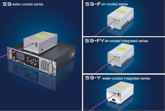
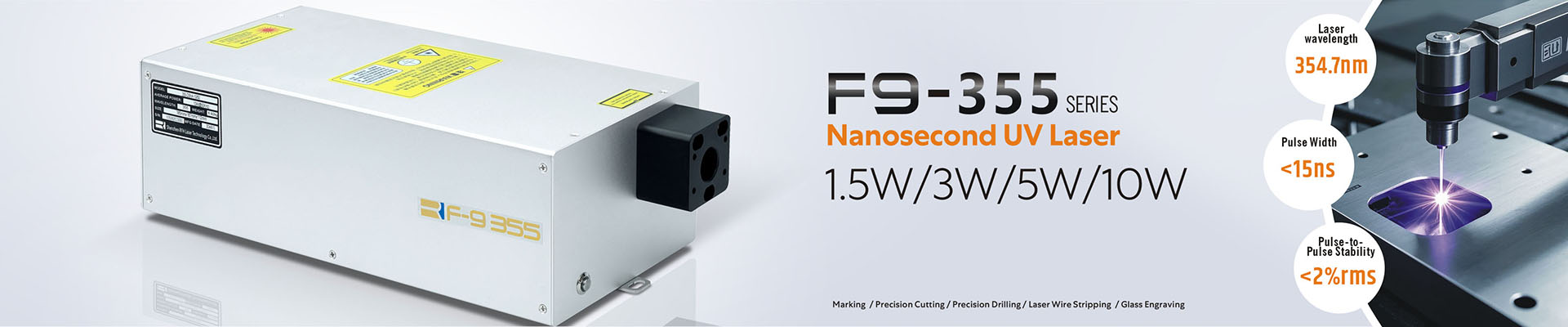
시장 수요를 충족하기 위해 RFH는 2020년에 S9 시리즈 UV 레이저를 새로 개발했습니다. S9 시리즈 UV 레이저는 동급 제품과 비교할 때 견고한 밀봉 캐비티, 매우 작은 크기, 단순하고 견고하며 높은 안정성, 고효율, 높은 신뢰성 및 우수한 레이저 기능을 갖추고 있습니다. 빔 품질. 컴팩트한 디자인으로 큰 광로를 구축할 필요가 없어 공간과 비용을 크게 줄이고 UV 레이저 마킹 기계 에 쉽게 설치할 수 있습니다 . 또한 S9 시리즈 캐비티 구조는 안정성과 확장성이 뛰어나 동일한 레이저 캐비티가 다중 출력 레이저를 생산할 수 있으며 다양한 출력 범위의 안정성이 크게 향상되었습니다.