Nanosecond Lasers 냉각 소스와 PCB 전용 CO2 레이저 장비의 차이점
Jun 27 , 2022The difference between Nanosecond Lasers cooled source and PCB dedicated CO2 laser equipment
The 2020 South China Advanced Laser and Processing Application Technology Exhibition will be held at the Shenzhen International Convention and Exhibition Center (Bao'an New Hall) from November 3 to 5. Under the premise of covering the core resources of the entire industrial chain of electronic intelligent manufacturing, the exhibition will focus on 5G and The theme of new infrastructure, driving new demands, and triggering new scenarios will explore the application of lasers in PCB, lithium battery, consumer electronics, microelectronics, medical and other fields, aiming to bring the audience an updated and more refined laser application exchange platform.
This issue of Radium Sir will take you to know in advance the exhibitors and exhibits that can apply laser processing technology to PCB circuit board processing at the South China Laser Exhibition, as well as their recommended exhibits suitable for PCB circuit board processing. Before visiting the South China Laser Exhibition, you must not miss these fairy companies. ■ TIPS
PCB (Printed Circuit Board), the Chinese name is printed circuit board, also known as printed circuit board, is an important electronic component, electronic component support and electrical connection carrier. Because it is made using electronic printing, it is called a "printed" circuit board.
uv laser | green laser | Ultraviolet lasers | uv dpss laser | nanosecond laser | UV laser source | Solid State Lasers
Almost every electronic device, ranging from electronic watches and calculators, to computers, communication electronic equipment, and military weapon systems, as long as there are electronic component systems with integrated circuits, in order to make electrical interconnections between various components, PCBs are used. plate. In the process of producing PCB boards, in order to improve the efficiency and yield, the processors first produce the whole board in a large area, and then cut it into small pieces during the use process, and the specific and important processing One way is laser processing.
In the past ten years, PCB circuit boards have been increasingly used in the fields of consumer electronics and automotive electronics such as mobile phones. The cutting edge has no dust, no burrs, no deformation, and no edge components are affected. basic requirements. The traditional processing mode often affects the performance of the PCB circuit board to varying degrees, or generates stress, dust and other harmful tiny particles during processing or causes static electricity to affect the performance of the circuit board. In contrast, laser cutting, laser marking and other processes stand out among the many processing modes of PCB boards because of their non-contact processing methods, small processing gaps, and no harmful tiny particles and static electricity. Favored by major PCB manufacturers.
Coherent (Beijing) Commercial Co., Ltd.
- Coherent Inc. -
■ Laser Intelligent Manufacturing Innovation Exhibition Area 12H59
Company Introduction Coherent, founded in 1966, is a world-renowned supplier of lasers and laser technology, serving scientific research, business and industry. Coherent spans the globe and is headquartered in the heart of California-Silicon Valley, providing a unique portfolio of products and services for research, life sciences, microelectronics and materials processing.
Products AVIA LX Lasers
product description
With the continuous development of ultra-thin and miniaturized 3C electronic devices such as smartphones, in order to achieve the goals of less space, faster speed and higher performance, electronic products have a more prominent demand for high-density PCBs. The requirements of "light, thin, short and small" are constantly increasing. In order to achieve this goal, multilayer boards gradually dominate the market, and the circuit layout of the PCB board needs to be closer to the edge of the board. Both of these requirements pose challenges to PCB cutting. How to improve the edge quality of cutting, reduce the heat-affected zone, and reduce the width of the incision while ensuring production capacity and not increasing the cost has become a technical challenge in the PCB processing process.
When using traditional lasers to cut thick plates, it is generally necessary to reserve a V-groove to avoid interruption of the optical path during the cutting process and reduce the laser power and affect the cutting efficiency. When cutting with Coherent's AVIA LX laser, pulse energy up to 400μJ can be fully utilized to scribe repeatedly along the same line, no V-grooving is required, so the cutting speed is faster and the kerf width is significantly reduced.
Features
■ Cost-effective, high-yield, high-efficiency, high-quality and stable
■ Can effectively reduce heat affected zone, improve cutting edge quality, reduce kerf width and increase production
■ AVIA LX works with virtually any existing PCB material, including fiberglass materials
Product advantages
Cut cross-sections of 1.6 mm thick multilayer PCBs with fiberglass layers using a competitor's UV solid-state laser and a Coherent AVIA LX laser, which has narrower trench channels and smaller HAZs.
Top view of a 0.95mm-thick PCB cut using a competitor's UV solid-state laser and Coherent's AVIA LX laser with a narrower, more consistent cut.
For lasers with lower pulse energies, the beam focus must be constantly moved as the beam penetrates the material, so that the minimum size of the focus always precisely matches the depth of cut in order to obtain a laser flux above the material ablation threshold. However, in the actual processing process, it is necessary to move the PCB board, or additionally use a three-axis scanner with focusing function. Either method will greatly affect the overall processing efficiency and schedule, increasing equipment costs and operational complexity.
The AVIA LX utilizes Coherent's advanced laser pulse timing and spatial positioning technology, which avoids heat generation in the substrate to a certain extent, eliminates thermal damage, and allows greater use of the high pulse of the laser when cutting thicker materials. energy. The high pulse energy of AVIA LX increases the laser focusing tolerance of the work surface. During the cutting process, the laser light source only needs to focus on a point in the middle of the PCB; at the same time, the high pulse energy of AVIA LX ensures that there is enough laser flux for ablation, As a result, the cutting speed can be accelerated, and the entire operating system is also very simple and convenient.
Features
Compared with traditional processes, laser PCB board coding has better accuracy and flexibility, which can make up for the shortcomings of traditional process processing, greatly improve production efficiency and yield, reduce costs and reduce pollution.
Applications
At present, it has been widely used in many fields such as digital products, wearable devices, and automotive circuit boards.
Product 1
PCB CO2-FTW055 Flying Marking System
product description
■ The equipment is directly connected to the PCB production line, and can be installed after developing (printing→exposure→developing→on-the-fly coding→post-baking) or other positions, mainly for marking characters. The equipment adopts the flying marking method. The PCB board flows into the equipment through the assembly line, and flows out of the equipment after flying marking. The PCB board does not need to stop during the whole process. Large marking range: 620*730mm. More than 160 groups of characters can be marked at one time (6 characters per group)
Applications
■ Cutting and drilling of hard and brittle materials: glass, sapphire, ceramic
■ Flexible material cutting, drilling: FPC, OLED, LCP
■ Special fine micromachining
Product 2
Large format PCB marking system (CO2-PCB650)
product description
■ It can mark characters, one-dimensional codes, two-dimensional codes and other small carts to automatically load and unload, and the multi-channel independent vacuum adsorption design ensures the stable loading and unloading of porous large boards. High precision, barcode gun automatically calibrates precise XY servo system, stable operation and fast speed
■ Laser configuration: CO2, green light 10W, UV optional
Features
■ Single wavelength output: 1064nm, 532nm, 355nm, 266nm
■ Output power: IR》100W, GR》50W, UV》40W, DUV》5W Support burst mode and PSO mode
■ Can meet the requirements of industrial 7x24 hours continuous operation
Applications
■ Cutting and drilling of hard and brittle materials: glass, sapphire, ceramic
■ Flexible material cutting, drilling: FPC, OLED, LCP
■ Special fine micromachining
Shenzhen Ruifengheng Laser Technology Co., Ltd.
- Shenzhen RFH Laser Technology Co., Ltd. -
■ Booth No. 12H75
Product 1
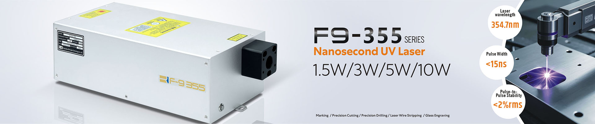
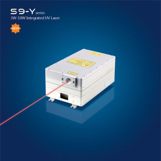
3W-10W S9 Pulsed Ultraviolet Solid State Laser-2020 New Products
product description
시장 개발의 요구에 따라 Shenzhen Ruifengheng Laser Technology Co., Ltd.가 2020년에 새로 출시한 S9 시리즈 펄스형 자외선 고체 레이저는 유사 제품보다 크기가 더 작고 디자인이 더 정교하며 광 출력이 더 안정적입니다. . 작고 콤팩트한 디자인은 사용자가 광 경로를 크게 만들 필요가 없어 비용을 크게 절감하고 공간을 절약할 수 있으며 플라잉 마킹 장비 분야에 쉽게 설치할 수 있습니다. S9 UV 레이저는 크기가 작을 뿐만 아니라 유사한 제품보다 더 안정적인 캐비티 구조와 더 강한 확장성을 가지고 있습니다. 동일한 캐비티는 다양한 파워의 레이저를 생성할 수 있으며 다양한 파워 세그먼트의 안정성이 크게 향상됩니다.
제품 특징
작은 크기, 고정밀, 높은 안정성
해결책
플라잉 조립 라인 마킹 분야를 위한 솔루션 제공
응용 분야
소비자 가전/반도체/PCB/의료/리튬 배터리/자동차 전자/산업용 전자
제품 2 35W 그린 레이저
제품 설명
Shenzhen Ruifengheng Laser Technology Co., Ltd.에서 개발 및 생산한 Expert III 532 시리즈 수냉식 녹색 반도체 펌프 펄스 고체 레이저는 35W의 출력을 가집니다. 이 시리즈의 레이저는 유리 마킹, 박막 에칭, 금속 산화물 층 파괴 등과 같은 대부분의 금속 및 비금속 재료의 표면 처리에 특히 적합합니다. 고전력, 고정밀, 높은 안정성
제품 특징
고출력, 고정밀, 고안정성
해결책
고출력 PCB 절단, 유리 조각 솔루션 제공
응용 분야
소비자 가전/반도체/PCB/의료/리튬 배터리/자동차 전자/산업용 전자
제품 설명
■ 강력하고 신뢰할 수 있는 긴 서비스 수명
■ 경량 설계
■ 반복 주파수 0~500kHz, 고반복 주파수에서 안정적인 고출력
■ 우수한 빔 품질
애플리케이션
PCB/FPC, 유리, 웨이퍼, 태양전지, 특정금속재료
제품 1 산업용 유사 동축 비전 Galvo
제품 특징
■ 마킹 그래픽의 위치를 조정하는 템플릿 동적 위치 지정(마크 포인트 보정)
■ 이미지 외곽선 추출 및 마킹
■ 이미지 캡쳐 및 부분 이미지 마킹
■ 임의의 각도, 임의의 수량, 제품 자동인식으로 지정된 위치에 정확하게 마킹
■ 작은 왜곡 렌즈, 교정을 피하기 위한 작은 왜곡.
■ Fiber, CO2, 자외선, 녹색광 등 다양한 파장의 레이저와 함께 사용 가능.
응용 분야
가전제품/PCB/자동차 전자제품/산업용 전자제품
제품 2 산업용 거리 측정기 Vision Galvo
제품 특징
■ 마킹 그래픽의 위치를 조정하는 템플릿 동적 위치 지정(마크 포인트 보정)
■ 이미지 외곽선 추출 및 마킹
■ 이미지 캡쳐 및 부분 이미지 마킹
■ 시각적 마킹, 마킹 크기, 범위 및 위치를 볼 수 있음
■ 임의의 각도, 임의의 수량, 제품 자동인식으로 지정된 위치에 정확하게 마킹
■ 검류계의 자동 미세 보정 지원
■ Fiber, CO2, 자외선, 녹색광 등 다양한 파장의 레이저와 함께 사용 가능.
응용 분야
소비자 가전/PCB/의료/리튬 배터리/자동차 전자/산업용 전자
해결책
레이저 마킹은 현대 제조, 특히 정밀 가공 및 미세 가공 분야에서 중요한 가공 방법이 되었습니다. 레이저 마킹은 고에너지 밀도의 레이저를 사용하여 공작물의 일정 부분을 조사하여 표면 재료의 색상을 기화시키거나 변화시켜 영구적인 마킹을 남기는 마킹 방법입니다. 레이저 마킹은 다양한 문자, 기호 및 패턴 등을 인쇄할 수 있으며 문자 크기는 밀리미터에서 마이크로미터까지 다양하므로 제품의 위조 방지에 특히 중요합니다. 초점을 맞춘 후 매우 미세한 레이저 광속은 물체 표면의 재료를 한 점 한 점 제거할 수 있는 도구와 같습니다. 고급 특성은 마킹 프로세스가 비접촉 처리로 기계적 압출이나 기계적 응력을 발생시키지 않는다는 것입니다. 그래서 그것은 처리된 품목을 손상시키지 않을 것입니다; 그리고 레이저 집광 크기가 작고 열영향 면적이 작고 가공이 미세하기 때문에 기존 방법으로는 달성할 수 없는 일부 공정을 완료할 수 있습니다.
기존의 레이저 마킹기는 일반적으로 공작물의 위치를 감지하는 기능이 없으며 고정 장치를 사용하여 위치 지정, 즉 수동 개입 및 위치 지정을 수행합니다. 그러나 미세하거나 극히 작은 가공물을 마킹할 때 정밀한 포지셔닝을 달성하기가 매우 어렵고, 가공물을 픽 앤 플레이스하기가 어렵습니다. 인적 요소 외에도 실제 작업에서 마킹 위치의 정확성과 일관성을 보장하는 것은 어렵습니다. 섹스. 고정구의 정확도에 의한 제품 가공의 위치는 부품의 마킹 위치 정확도에 직접적인 영향을 미치며 각 가공 대상의 좌표 위치는 고유합니다. 동시에 밀리미터 수준 이하의 물체를 가공하는 마킹 효과는 육안으로 구분할 수 없으며,