10W UV 레이저 절단기에 웨이퍼 절단을 선택하는 이유는 무엇입니까?
Oct 18 , 2021
Most semiconductor materials of ultraviolet laser cutting machine have good absorption of light in the ultraviolet band. Take the absorption of monocrystalline silicon in different wavelength bands as an example. When the semiconductor material is processed by laser in the ultraviolet band, due to the narrow focus spot of ultraviolet light, The photon energy is relatively high and can break the chemical bond of the material. The volume of the space occupied by the product expands rapidly, and finally shoots and separates the parent body in the form of a bulk explosion and takes away the excess energy. The hot zone has little effect. In this process, since there is no heat generated, the process of ultraviolet laser is also called "cold working". After the cutting is completed, each chip is separated by the corresponding split process. In this way, the machine can be used effectively, and at the same time, it can be convenient for us to find the fault in the maintenance of the problem, and facilitate the maintenance.
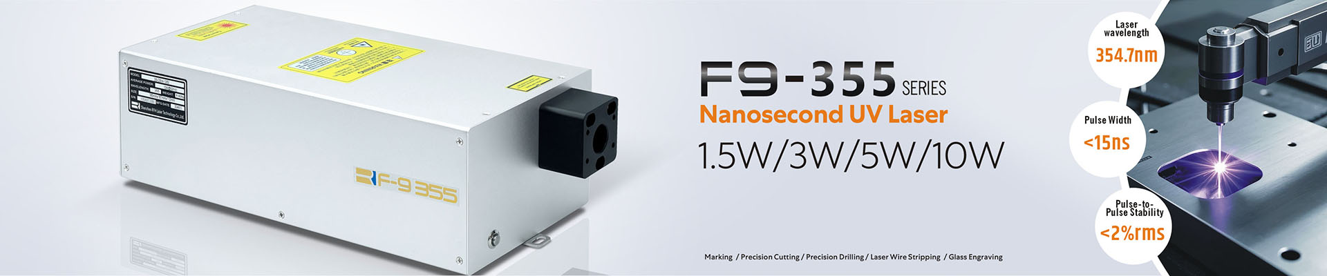
355nm UV laser cutting machine
Because the energy of this special wavelength and frequency laser acting on the material to be processed is only a few watts or even milliwatts, there is no molten material on the outside or inside, and the front and back sides are almost invisible with the eyes. , This provides a larger space for chip manufacturers to reduce the width of the cutting channel and increase the number of chips per unit area to reduce costs. Since the short-wavelength ultraviolet laser has almost no thermal damage, the material does not need to be cooled, and the entire cutting process is performed in a completely dry environment. The molten material is also vaporized, so the appearance of the material is not contaminated at all, which also solves the problem of contamination of semiconductor wafers.
자외선 레이저 | 녹색 레이저 | 자외선 레이저 | 자외선 dpss 레이저 | 나노초 레이저 | UV 레이저 소스 | 고체 레이저
UV 레이저의 적용이 점점 더 대중화되고 있습니다.
현재 자외선 레이저의 점진적인 성숙과 안정성으로 인해 레이저 가공 산업은 적외선 레이저에서 자외선 레이저로 전환되었습니다. 동시에 자외선 레이저의 응용이 점점 더 대중화되고 있으며 레이저 응용 분야는 더 넓은 분야로 이동하고 있습니다. UV 레이저 절단기의 작동 원리는 UV 레이저 웨이퍼 절단입니다. 사파이어 기판의 표면은 단단합니다. 일반적으로 커터 휠은 절단하기 어렵고 마모가 크고 수율이 낮으며 절단 경로가 30μm보다 커서 사용 면적이 줄어들뿐만 아니라 제품의 생산량도 줄어 듭니다. 청색 및 백색 LED 산업에 힘 입어 사파이어 기판 웨이퍼 절단에 대한 수요가 크게 증가했습니다.
반도체 칩 가공 분야에서의 UV 레이저 적용
실제로 반도체 칩 가공 분야에서 자외선 레이저의 적용은 주로 칩 절단, 웨이퍼 미세 홀 드릴링, 웨이퍼 마킹, 박막 저항의 레이저 조정, 레이저 측정, 레이저 에칭, 심자외선 프로젝션 리소그래피 등을 포함합니다. 이러한 응용 분야에서 대규모 생산의 지속적인 발전에 적응하기 위해 출력 및 비용 측면에서 전통적인 다이 분리 기술은 더 이상 실용적이지 않으며 자외선 레이저 절단 기술은 큰 잠재력을 가진 응용 프로그램이 될 것입니다. 응용 프로그램의 핵심 기술. 또한 이 기술의 성공을 더욱 확신하게 되었습니다.