자외선 레이저 355nm는 무엇입니까
Feb 07 , 2023Ultraviolet laser is a laser that produces ultraviolet beam, which is mainly divided into gas ultraviolet laser and solid ultraviolet solid laser.
Under the action of the pump source, the working medium is reached by absorbing the external energy. After the number of particles reversed by the number of particles is greater than the loss, the light is enlarged. Some of the enlarged light feedback continues to motivate to generate oscillations in the resonant cavity.
The gas medium mainly uses pulses or electron beam discharge. Through the mutual collision between electrons, the gas particles are excited from low energy levels to high energy levels to generate excitement to obtain ultraviolet laser.
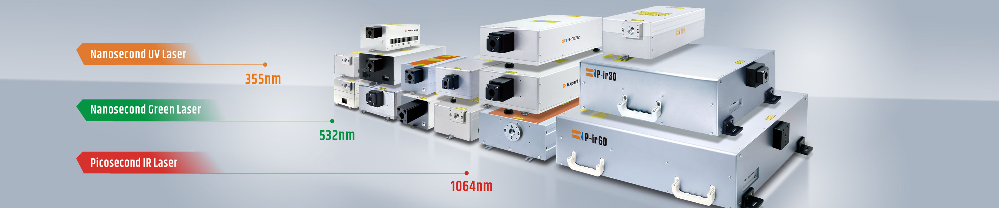
The solid medium is an ultraviolet laser that radiates outward by a non -linear frequency crystal in a frequency conversion of one or above. Standards and all -solid -state ultraviolet laser are often used for laser processing and treatment. The classification of ultraviolet laser is shown in the table below.
There are many advantages in ultraviolet laser processing, which is also the first choice technology in the development of scientific and technological information. First of all, ultraviolet laser can output ultra -short wavelength laser, which can accurately handle ultra -small and fine materials; secondly, the "cold treatment" of ultraviolet laser will not destroy the material itself as a whole, but it is processed on its surface; there is basically no heat damage effect; some materials have some materials; The visible light and infrared laser cannot effectively absorb the irreplaceable process. The advantage of ultraviolet is that basic materials are widely absorbed by ultraviolet light. UV laser, especially solid ultraviolet laser, has a compact structure and small size, simple and easy to maintain, and easy to produce. UV laser is widely used in processing medical biomedical materials, criminal case evidence collection, integrated circuit board, semiconductor industry, micro -light component, surgery, communication and radar, laser processing cutting very widely.
Change the surface characteristics of biological materials
In some treatments, many medical materials need to be compatible with human tissue, or even repair, such as ultraviolet laser treatment of internal diseases and rabbit corneal experiments. Sometimes they need to change biomromes characteristics and macromolecular structures. For good pulse parameters, the experiments will use 100 nm, 120 nm, and 200 nm to illuminate the surface of the medical biological materials to improve the physical chemical structure of the surface of the material, and does not change the overall chemical structure of the material. , Make the processing organic biological materials and human tissue compatibility and hydrophilicity significantly improved, and it is very helpful in medical and biological applications.
Criminal investigation
In the field of criminal investigation, when it is found that fingerprints have a unique characteristics as DNA, fingerprints can be printed as an important biological certificate left by criminal cases as criminal cases.
The old method can cause sample damage, and it is difficult to collect and store evidence. The current research is based on the surface fingerprints of non -permeability objects, such as tape, photos, and glass. "Ultraviolet Lighting Imaging Technology" and "UV laser reflection imaging technology", that is, the potential fingerprints of ultraviolet laser irradiation with a wavelength of 266 nm, observed and recorded UV lasers through 266 nm and 340 nm pass filter lights, respectively Test and adopt collection.
70 percent of the 120 experimental samples in the experiment can be successfully tested. UV short wave technology has improved the success rate of potential fingerprints, and it is convenient and fast and easy to control its optical characteristics. It has a large application prospect in the field of court science. UV detection can be detected by common biological tests such as salivary spots, shedding cells, blood stains, and hair follicles.
However, the ultraviolet laser with a short wave 266 nm at a fixed distance is analyzed through the long -ray biological examination materials at different times to analyze the DNA for analysis. It was found that the ultraviolet laser of short wave 266 nm was seal, blood stains, saliva, shedding cells, and hair follicles. 5 common types of hair. The results of the DNA test of biological evidence have a serious impact, but the detection of biological DANs such as hair follicles, body fluid saliva, and blood spots on hair has only a small number of biological DAN.
Short -wave ultraviolet laser will have an impact on some DNA biological examinations, so when the criminal investigation survey is obtained, it is necessary to carefully choose the extraction method based on evidence.
Application of UV laser on the integrated circuit board
In the production process of a variety of circuit boards in the industrial field, from the beginning of wiring to the production of micro -precision embedded chips that require advanced technology, the flexible circuit, polymer and copper layer circuit in the integrated circuit board need Drilling micropores and cutting, including the repair and detection of materials on the circuit board, often need to be used for fine processing and processing. Laser micro -processing technology in circuit board processing is obviously a better choice.
During the processing process of laser, the working machine does not contact the processed product, effectively avoids mechanical force, rapid processing, high flexibility, and no special requirements for working occasions. The following magnitude.
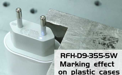
The more traditional drilling method on the circuit board is to use ultraviolet laser and CO2 laser for non -metal marking (CO2 laser with a wavelength of 10.6 μm for non -metallic material marking; wavelength 1064 nm or 532 nm is generally used for metal metal Material marking).
At present, ultraviolet laser machining technology can be used, which can achieve micron -level processing, high accuracy, can make ultra -fine zero devices, and can be applied to laser beams with less than 1 μm spots.
However, the CO2 laser mainly hit the holes of 75 ~ 150 mm, and the small holes are prone to misplaced, while ultraviolet laser can hit holes of less than 25 mm, high accuracy and not misplaced.
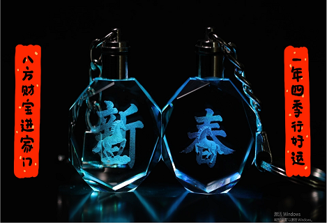
Processing and preparation of microcomioxito device
In the information age of the rapid development of science and technology and modern industries, to build more experimental systems in smaller space and achieve more functions, it is necessary to speed up the development of information technology. Small, miniaturized, and only complete device processed on the surface chemical keys of the material.
It has important application and research value in the fields of military radar communication, medical treatment, aerospace and biochemistry. It can be deepened and optimized, and developed on nano -scale micro -optical elements to transform traditional optical components' functions and characteristics.
Micrological components have the advantages of easy mass production and easy realization of formation, and simple and light and flexible, but its main materials are quartz glass.
In the process of application and treatment, quartz glass is easy to produce cracks and pit, which is a hard and brittle material, which greatly weakens its optical properties.
Therefore, the direct writing "cold" processing technology of ultraviolet laser improves the efficiency of microdegenene device, quickly completes the processing of micro -light components with high -precision micro -structures and does not hurt the material. It can flexibly complete the processing of different needs of large size.
Foreign scientific research institutions have studied the earlier research of ultraviolet -ultraviolet processing silicon wafers, and then they started to study the cutting technology and cutting surface of the silicon wafer cutting technology later.
Application of UV laser in the semiconductor industry
최근 몇 년 동안 자외선 레이저는 반도체 재료의 미세 가공에 점점 더 많은 관심을 끌었습니다. 수천 개의 고밀도 회로 부품은 집적 회로에서 매우 일반적이므로 일부 고정밀 처리 및 처리 방법이 필요합니다. 실리콘과 사파이어와 같은 반도체 재료와 같은 반도체 재료와 같은 일부 고품질 기기 및 장치도 있습니다. UV 레이저를 이용하여 필름의 분광 특성을 연구합니다. 동시에 자외선 레이저는 실리콘 재료의 활용률을 높일 수 있으며 실리콘 표면의 미세 구조를 변경할 수 있어 2차원 미세 광 그리드와 같은 태양 전지 패널의 개발에 도움이 됩니다. 등 에센스
이러한 수십 년간의 개발 및 연구를 통해 자외선 레이저의 기술과 응용 분야는 점점 더 광범위하고 성숙해지고 있습니다. 표면에 미세가공 및 가공을 하면서도 대상물의 물성이 변하지 않는 정밀한 "냉간" 가공기술을 가지고 있습니다. 통신, 광학, 군사, 범죄 수사, 의료 등 다양한 산업 및 분야에서 널리 사용되고 있습니다.
점점 더 새로운 유형의 주파수 결정 및 이득 매질이 출현함에 따라 파장이 짧은 자외선 레이저가 짧을수록 자외선의 출력이 높아 향후 더 많은 산업에 적용되어 다양한 산업 및 가공 분야의 자외선 레이저는 훨씬 더 지능적이고 효율적이며 정확하고 높은 반복 및 높은 안정성이 미래 발전 추세입니다.