PCB에서 레이저를 사용하는 방법
Dec 26 , 2022The manufacturing of PCB is a very complex task that requires using specialized equipment and engineering expertise. The advancement in technology has streamlined the major aspects of PCB manufacturing, with the introduction of lasers being one of the most recent developments.
The fabrication of PCBs requires various materials. These materials are selected based on their electrical performance to ensure mechanical and electrical reliability. PCB laser etching plays a significant role in the manufacturing of PCB.
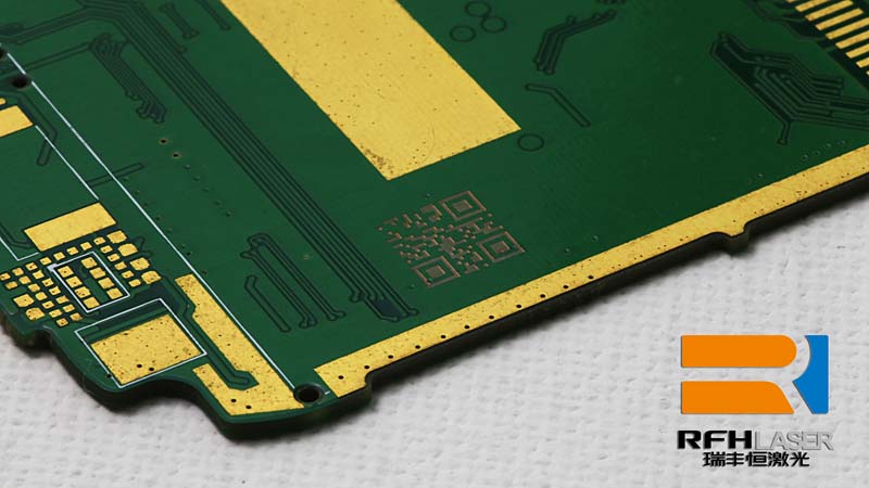
PCB laser is used for marking circuit boards, an important step in PCB manufacturing. Since electronics manufacturing is becoming complex it is important to mark boards to determine major components and make sure that parts are placed in correct positions so that they can be well connected.

Identifying marks have become an important aspect in PCBs manufacturing. Traditionally, identifying marks are done alphanumerically, but there are restrictions due to the space available on the PCB surface. That is why lasers are used in marking PCBs since they can offer accurate marking.
Fiber laser PCB can help to include identifying codes to any PCB surface; they can use QR codes or bar codes to cram information into a smaller space.
Lasers are also very fast when it comes to marking PCBs. They can etch codes in a few seconds while preventing the material around the area of application from any damage or distortion. Laser marking also provides information in the manufacturing of integrated circuits. In this application, precision, efficiency, and precision are very important.
It is also important to know that using lasers to mark printed-board-circuits correspond with the marking of components by using the same procedure. This makes it easy to trace and replace parts while making sure that sensitive and fragile parts aren’t placed under undue pressure.
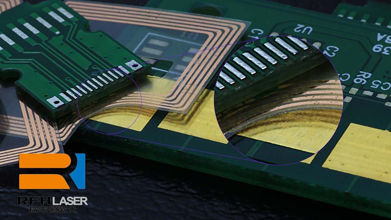
Cutting is an important aspect of PCB production since a circuit board requires to be designed using a stencil with apertures to connect and solder components. A fiber laser can be used to cut PCB stencils in large volumes within a few seconds. The beam of a laser cut pcb can punch through the circuit board material to leave the necessary apertures thereby ensuring that it doesn’t compromise the integrity of the material surrounding it.

In the case of mass production, this process has to be done repeatedly. Cnc laser pcb prevents damages from occurring and minimizes waste since they use a non-contact approach to cut materials. Laser cut fr4 are an important aspect of PCB manufacturing.
Lasers Sintering in PCBs
Sintering is considered the perfect solution to affixing components of PCBs and this method can overcome the problems of soldering and enable more durable, stronger, and consistent bonds to form during the manufacturing of PCBs.
Laser sintering is giving opportunity for the development of cutting edge PCBs which are created without solder. High-density circuits are suitable for this technique, allowing improved stability. When sintering is done, a laser is applied to a powder that contains silver. The heat coming from the laser makes the powder reach a melting point and this is allowed to cool off to form a solid connection.
Laser depaneling in PCB is a great way for PCB producers to save time and money. Circuit boards contain sensitive parts that may get easily damaged and laser depaneling helps to reduce stress on these parts and their solder joints.
How to Select Laser Routing for PCB Depaneling
Laser routing is one of the popular approaches to depaneling. This procedure ensures that there is no physical contact with the board. Many producers consider laser routing to be ideal for sensitive and small PCBs used in the most recent wearable technologies.
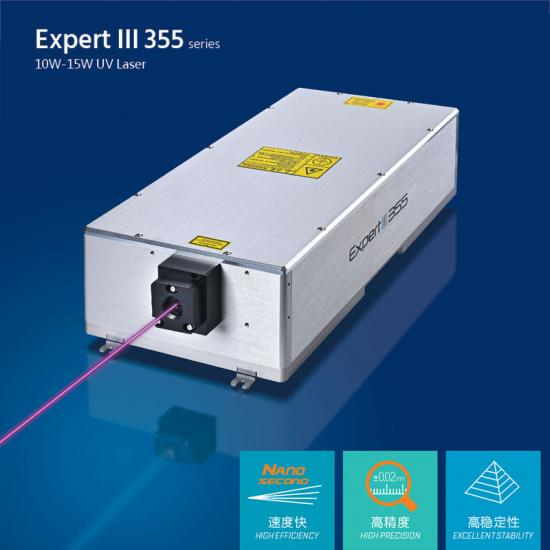
UV (355 nm wavelength) and CO2 (10.6µm wavelength) are the two lasers for PCB depaneling. The relative importance of cycle time and the neatness of the cut edge are the most important factors to consider when determining the type of laser to use.
Choosing the Right Laser Source
It is important you determine the appropriate laser source for your depaneling needs. CO2 and UV lasers have their disadvantages and advantages.
Lasers that involve UV use “cold” cutting technology. UV lasers make it easy to control the thermal charring of the edge. Therefore, a UV laser is a better option if reducing char is more vital than speed.

Pros
Delivers very clean cuts
Low HAZ
A narrow kerf width
Ability to cut copper leads accurately
Cons
Longer cut times
More expensive
When utilizing a UV laser to get clean cuts, several repetitions of laser scanning are utilized to singulate the PCBs. To control the cut speed, software controls are utilized. These cuts cut through the whole panel that cingulate the board.
CO2 Lasers
A CO2 laser is a preferable option if cycle time is very important. CO2 laser PCB can help to make full cuts and are more commonly used to create perforated cuts. Making use of the perforation technique helps to reduce char and as well as allows for easier load and unload of panels and boards from the cutting machine.
The gap left between perforations is a vital factor in the perforation technique. A bigger gap will lead to less char on the edge, but more force will be required to separate boards. We can easily adjust perforation strength based on the specifications given.
Furthermore, the amount of charring and cycle time increases as material thickness increases. If V-grooves can be used to manufacture panels at cut locations, laser cuts can be faster and cleaner.
Pros
Fast cut speeds
Allows processing of aluminum panels
Thicker substrates cut well
Lower cost for each watt
Cons
Larger HAZ
More charring on cut edges
More kerf width
How to Improve Cut Accuracy for PCB Depaneling
fiber laser pcb
When depaneling PCBs, the accuracy of the cut plays a significant role in reducing waste and damage. You must ensure there is consistent cut placement and this can be achieved by ensuring accurate alignment of the laser with panel components and features.
A vision system identifies certain features on the panel and adjusts the cut path to ensure the cuts align accurately to the circuits.
Why Laser Depaneling is Better Than Other Methods
Laser routing is a method that involves a no-contact process. This means that;
No mechanical stress on components
No sharpening or replacement of worn blades
Can cut through any path even curves
Software controls that enable simple and quick change between different cut patterns
No switching of mechanical parts or realigning of blades
Lasers Drilling in PCBs
Laser drilling makes holes on a printed-circuit-board to create connections between several layers. The electronic appliances we have in our homes consist of HDI boards that make use of laser drills. Laser drilling procedures guarantee accuracy even when working with small sizes.
Laser drilling utilizes laser energy for drilling a hole. This is totally different from drilling holes with a machine. Holes are drilled on PCBs for placing components and bringing interconnection between various layers. Lasers are capable of drilling between 2.5 to 3-mil vias on flat reinforced glass. It can drill about 1-mil vias when it comes to an unreinforced dielectric.
Benefits of Drilling with a Laser
There are several benefits of using lasers to drill and they are discussed below;
Precise control: Lasers help you gain control over the heat output, beam intensity, and the period of the laser beam. This provides high accuracy and helps to make various hole shapes.
Multi-tasking: Lasers can be used in several manufacturing processes like cutting, welding, sintering, etc.
Non-contact process: Lasers ensure a no-contact process and as such, there is no damage caused by drilling vibration.
High aspect ratio: The aspect ratio is an important parameter of a drilled hole. The aspect ratio is the ratio between the diameter of the hole and the drilled depth. Lasers offer a high aspect ratio since they can make holes with small diameters.
Factors to Consider During Laser Drilling
Some factors need to be considered during laser drilling, these two major factors should be considered;
The copper thickness
The lowest thickness of the target copper layer should be twice as thick as the top copper layer to be drilled. Lasers are the most effective way to make microvias in PCBs. Laser-drilled microvias are important in the manufacturing of PCBs
Non-homogeneity of the stack-up
While using lasers to drill, the non-homogeneity of the stack-up is very important. Several materials get energy at various rates. For instance, FR4 resin takes up energy at the exact rate as the glass fibers. BT epoxy resin vaporizes at a much faster rate than glass and as such, leaves glass fibers in the hole.
Conclusion
레이저는 PCB 제조에 사용되는 중요하고 특수한 장비입니다. 이 장비는 여러 용도로 사용되며 PCB 드릴링, 절단, 마킹 및 소결에 사용됩니다. 정밀도를 제공하기 때문에 이 장비는 PCB 제조업체에게 선호되는 옵션입니다. 레이저는 또한 비접촉 방식을 활용하여 PCB 생산에 쉽게 사용할 수 있습니다. 레이저 조각 PCB는 PCB 생산에 사용됩니다.