싱가포르 고객 구매 자외선 355nm dpss 레이저 소스 절단 알루미나 세라믹 기판
Dec 08 , 2022Ultraviolet 355nm dpss Laser source cutting alumina ceramic substrate
In the production of printed circuit boards, the substrate mainly plays the role of mechanical support protection and electrical interconnection (insulation). Alumina ceramics are one of the most popular substrate materials due to their heat resistance, high mechanical strength, wear resistance, high temperature resistance, low dielectric loss, smooth surface and low porosity.

Alumina ceramics is a ceramic material mainly composed of alumina (Al2O3), and alumina ceramic substrates can also be called ceramic wafers. Due to the hard and brittle characteristics of alumina ceramics and the development of electronic packaging technology in the direction of miniaturization and high density, the cutting requirements for substrate materials are getting higher and higher.
With the development of laser technology, lasers have also appeared in the process of cutting alumina ceramic substrates. Compared with traditional waterjet cutting and mechanical cutting methods, the important advantage of laser cutting is that it avoids the cost and long cycle of manufacturing molds, and has high efficiency, better flexibility, less edge chipping, and more consistent processing results in the same batch . At the same time, the non-contact processing of laser cutting can avoid the damage of external mechanical stress to the material, and also solve the flaws of the traditional cutting process.
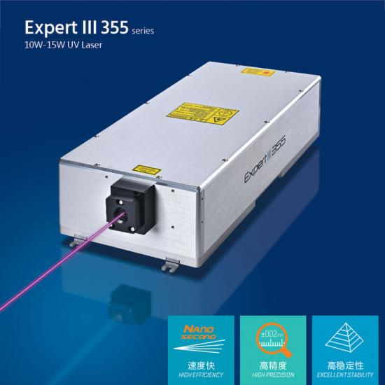
Ultraviolet 355nm dpss Laser source for non-contact "cold" processing of alumina ceramic substrates. When the 355nm ultraviolet light is highly focused and acts on the local surface of the substrate, the surface material quickly absorbs heat energy, causing the temperature to rise sharply, melt and vaporize, and with the help of auxiliary gas blowing, the effect of removing the surface material of the material is achieved. Then, the optical path is set in the cutting path The guided kerf is gradually formed over time, and then the section is formed, and the cut is finally completed. Due to the high single-photon energy of 355nm ultraviolet light, most materials have a higher absorption peak at 355nm wavelength, coupled with the small pulse width (about 25ns), the whole process has a small thermal effect and a small HAZ range, so it is called cold processing, thus Obtain the processing effect with higher cutting surface quality and high yield rate.
또한, 자외선 355nm dpss 레이저 소스는 빔 품질(M2<1.2)이 우수하고 초점이 양호하며 초점이 맞춰진 지점의 직경이 미크론 수준이라는 특성도 있습니다. 알루미나 세라믹 기판을 절단할 때 커프가 작아 원자재를 절약하고 기업의 비용을 더욱 절감할 수 있습니다. 또한 다양한 형상 요구 사항에 따라 컴퓨터를 통해 도면을 출력한 후 고속 절단을 수행하여 생산량을 높일 수 있습니다.

자외선 355nm dpss 레이저 소스는 알루미나 세라믹 기판의 후속 드릴 공정에도 적용할 수 있다는 점을 언급할 가치가 있습니다. 공정 매개변수의 설정을 통해 기판 재료를 점 단위, 라인 단위 및 레이어 단위로 높은 제어 가능성으로 처리할 수 있습니다. 관통 구멍이나 구멍이 다른 막힌 구멍 또는 사각형 구멍과 같은 기타 그래픽을 처리할 수 있습니다. 테이퍼는 제어 가능하고 유연합니다. 강력한 성능, 빠른 속도, 높은 정밀도 및 우수한 안정성.