PCB 시장이 고출력 나노초 UV 레이저에 성장 모멘텀을 가져올 수 있는 이유
Aug 23 , 2022PCB 시장이 고출력 나노초 UV 레이저 에 성장 모멘텀을 가져올 수 있는 이유
2019년에는 레이저 가공 시장의 성장률이 더욱 둔화되었습니다. 일부 애플리케이션 시장의 성숙도와 홍해에서의 경쟁으로 인해 관련 회사는 운영 압박 증가와 실적 저하라는 딜레마에 직면하게 되었습니다. 2020년 새로운 크라운 폐렴 전염병은 레이저 회사의 발전을 가져왔습니다. 가려진. 이러한 환경에서 OFweek Laser Network는 PCB 가공과 관련된 레이저 시장이 여전히 성장하고 있음을 발견했습니다. 일부 상장사에서 공개한 자료에서도 PCB 사업 수주가 실적 성장을 뒷받침하는 주요 동력이 됐다. PCB 시장의 발전은 어떻습니까? 그리고 레이저 회사에 엄청난 성장 모멘텀을 가져다 줄 수 있는 이유는 무엇입니까?
PCB 및 FPC 산업의 급속한 발전, 거대한 시장 증가
PCB는 인쇄 회로 기판의 약자입니다. 전자 산업의 중요한 구성 요소 중 하나이며 거의 모든 전자 제품에 사용됩니다. 주요 기능은 다양한 구성 요소 간의 전기적 상호 연결을 실현하는 것입니다. 인쇄회로기판은 전자부품의 조립 및 납땜을 위한 절연기판, 연결와이어, 패드로 구성되어 있으며, 도체회로와 절연기판의 이중기능을 가지고 있다. 제조 품질은 전자 제품의 신뢰성에 직접적인 영향을 미칠 수 있습니다. 오늘날 전자정보제품 제조업의 기초산업이며, 현재 글로벌 전자부품 소분산업에서 가장 생산가치가 큰 산업이기도 하다.
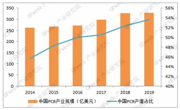
PCB의 응용 시장은 가전, 자동차 전자, 통신, 의료, 군사, 항공 우주 등을 포함하여 매우 넓습니다. 현재 소비자 가전 및 자동차 전자 제품의 급속한 발전은 PCB 응용 분야의 주요 분야가 되었습니다. 오랫동안 글로벌 PCB 출력 가치는 주로 북미, 유럽 및 일본에 집중되었습니다. 2000년 이후 PCB 산업의 초점은 아시아 지역, 특히 중국 시장으로 이동하기 시작했습니다. 2009년 중국 본토 PCB 산업의 생산액은 전 세계 생산량의 약 1/3을 차지했다. 2017년에는 50.5%에 도달하여 전 세계 PCB 출력 가치의 절반을 차지했습니다.
데이터 출처: Prismark, OFweek 산업 연구소
In 2019, affected by trade frictions, declining terminal demand and exchange rate depreciation, the global PCB output value declined slightly, but the Chinese market benefited from the rapid development of 5G, big data, cloud computing, artificial intelligence, Internet of Things and other industries, becoming the only one in 2019. growing area. According to Prismark data, the size of China's PCB market in 2019 was about US$32.9 billion, accounting for 53.7% of the world.
In the PCB application of consumer electronics, FPC develops the fastest, and its proportion in the PCB market continues to increase. FPC is the abbreviation of Flexible Printed Circuit, which is a highly reliable and reliable product made of polyimide (PI, also known as PI cover film in the industry) or polyester film as the base material. It is an excellent flexible printed circuit board with the characteristics of high wiring density, light weight, thin thickness and good bendability. Under the current trend of intelligent, light and thin mobile electronic products, FPC is widely used due to its advantages of high density, light weight, thin thickness, bending resistance, flexible structure, high temperature resistance, etc. the only solution.
The rapidly developing PCB market has fostered a huge derivative market. With the development of laser technology, laser processing has gradually replaced the traditional die-cutting process and has become an important part of the PCB industry chain. Therefore, in the context of the slowdown in the overall growth rate of the laser market, the PCB-related business can still maintain high growth.
The advantages of laser in PCB and FPC processing
The application of laser on PCB mainly includes cutting, drilling, marking, etc., especially cutting. Compared with the traditional die-cutting process, laser cutting is a non-contact process, without the need for expensive molds, and the production cost is greatly reduced; in addition, the traditional process is difficult to solve a series of problems such as burrs, dust, stress, and inability to process curves on the edge. The laser spot is only ten microns after focusing, which can meet the processing requirements of high-precision cutting and drilling, and solve a series of problems left in the traditional process. This advantage is catering to the development trend of precision circuit design, and it is an ideal tool for PCB, FPC, PI film cutting.
In fact, the application of PCB laser cutting technology in the PCB industry started earlier, but CO2 laser cutting was used in the early stage, which has a large thermal impact and low efficiency, and has not been able to achieve good development. It is only used in some special fields (such as scientific research , military, etc.) are used. With the development of laser technology, more and more light sources can be used in the PCB industry, and a breakthrough has been found for the industrial application of laser cutting PCB.
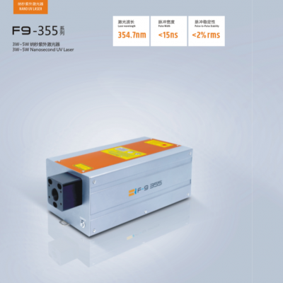
Currently, the lasers used in FPC and PI film cutting are mainly nanosecond solid-state UV lasers, and the wavelength is generally 355nm. Compared with 1064nm infrared and 532nm green light, 355nm UV has higher single-photon energy, higher material absorption rate, less thermal impact, and higher processing accuracy.
From a principle point of view, pulsed laser cutting materials can be divided into two situations: one is the photochemical principle, using the single photon energy of the laser to reach or exceed the chemical bond energy of the material to break some chemical bonds of the material to achieve cutting; the other is the light According to the physical principle, when the laser single photon energy is lower than the chemical bond energy of the material, the very high energy density at the focused spot exceeds the gasification threshold of the material, thereby instantly gasifying the material and realizing the cutting of the material. But in fact, when cutting FPC or PI film with UV laser, the principles of photochemical and photophysical cutting exist at the same time.
The following two processing principles are explained by taking PI film as an example. The bond energy of C-C bond and C-N bond in normal state is 3.45eV and 3.17eV respectively, while the single-photon energy of 355nm UV laser is 3.49eV, which is higher than that of C-C bond and C-N bond in normal state It can directly destroy the chemical bonds of materials. (Reference: Zhang Fei, Duan Jun, Zeng Xiaoyan, et al. Research on 355nm ultraviolet laser processing of blind vias in flexible circuit boards [J]. China Laser, 2009, 36(12):3143-3148.)
In the photophysical effect, there will be heat generation and accumulation, and the temperature of the material will continue to rise. When the temperature of the PI material is higher than 600 °C, the ratio of N and O elements will continue to decrease relative to the C element, and the final material is mainly dominated by the C element, that is, the material is carbonized. The diffusion distance formula L=[4Dt]^1/2, where D is the thermal diffusivity of the material, and t is the laser pulse width. (Reference: Zhang Peng, Chi Weidong, Shen Zengmin. Influence of high temperature carbonization on the structure and properties of polyimide (PI) thin films [J]. Carbon Technology, 2008, 27(6):10-12.)
It can be seen that when the material is constant, the larger the laser pulse width, the larger the diffusion distance of the thermal energy generated by the laser on the material, and the greater the thermal damage to the material. Therefore, the narrower the pulse width, the better the processing effect.
20W/25W nanosecond UV laser: higher power, better effect
As mentioned above, my country's PCB industry has benefited from the rapid development of emerging industries such as 5G and big data. The emergence of new industries and new technologies has also put forward higher requirements for the FPC and PI film cutting industries. In order to achieve less carbonization and faster efficiency, laser companies are also constantly making technological innovations, and constantly exploring higher frequencies, narrower pulse widths, and higher powers.
What kind of changes can the new high-frequency short-pulse-width nanosecond UV laser bring to PCB processing? The following shows some processing cases
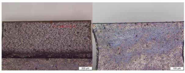
Gold finger cutting
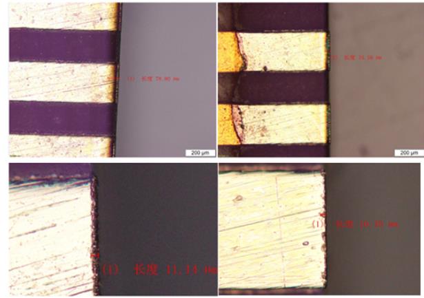
AWAVE 15W @50KHZ cutting effect, effective speed: 50mm/s (left)
FORMULA 15W @150KHZ cutting effect, effective speed 100mm/s (right)
Compared with the traditional AWAVE series laser, the cutting effect of the FORMULA series laser is significantly improved, and the cutting efficiency has also been improved by 100%.
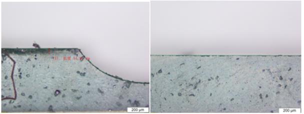
Copper Foil Drilling
Front (left) Back (right)
Drilling holes on the copper foil with a thickness of 100um, the efficiency of the 20W FORMULA series laser is 60% higher than that of the 15W, reaching 250 mm/s.
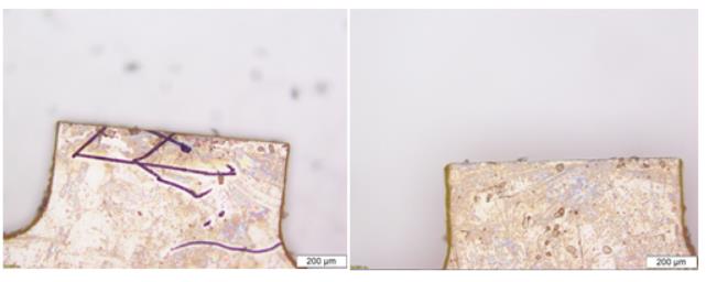
PCB cutting
Front not wiped (left) Back not wiped (right)
For PCB cutting with a thickness of 400um, the efficiency of the 20W FORMULA series laser is 50% higher than that of 15W, reaching 60mm/s.
FPC reinforcement board cutting
Front (left) Back (right)
For cutting FPC reinforced plate with PI thickness of 100um, the efficiency of 20W FORMULA series laser is 60% higher than that of 15W, reaching 250 mm/s.
image.png
Front (left) Back (right)

The 20W FORMULA series laser is 40% more efficient than 15W when cutting the FPC reinforced plate with a thickness of 130um, reaching 140 mm/s.